- 您现在的位置:买卖IC网 > Sheet目录3880 > PIC18F8621T-I/PT (Microchip Technology)IC PIC MCU FLASH 32KX16 80TQFP
PIC18F6525/6621/8525/8621
DS39612B-page 108
2005 Microchip Technology Inc.
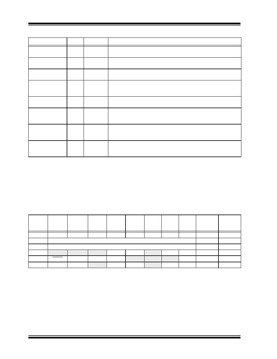
TABLE 10-3:
PORTB FUNCTIONS
TABLE 10-4:
SUMMARY OF REGISTERS ASSOCIATED WITH PORTB
Name
Bit#
Buffer
Function
RB0/INT0/FLT0
bit 0
TTL/ST(1)
Input/output pin or external interrupt input 0, ECCP1 PWM Fault input.
Internal software programmable weak pull-up.
RB1/INT1
bit 1
TTL/ST(1)
Input/output pin or external interrupt input 1.
Internal software programmable weak pull-up.
RB2/INT2
bit 2
TTL/ST(1)
Input/output pin or external interrupt input 2.
Internal software programmable weak pull-up.
RB3/INT3/
ECCP2(3)/P2A(3)
bit 3
TTL/ST(4)
Input/output pin, external interrupt input 3, Enhanced Capture 2 input/
Compare 2 output/PWM 2 output or Enhanced PWM output P2A.
Internal software programmable weak pull-up.
RB4/KBI0
bit 4
TTL
Input/output pin (with interrupt-on-change).
Internal software programmable weak pull-up.
RB5/KBI1/PGM
bit 5
TTL/ST(2)
Input/output pin (with interrupt-on-change).
Internal software programmable weak pull-up.
Low-Voltage ICSP enable pin.
RB6/KBI2/PGC
bit 6
TTL/ST(2)
Input/output pin (with interrupt-on-change).
Internal software programmable weak pull-up.
Serial programming clock.
RB7/KBI3/PGD
bit 7
TTL/ST(2)
Input/output pin (with interrupt-on-change).
Internal software programmable weak pull-up.
Serial programming data.
Legend: TTL = TTL input, ST = Schmitt Trigger input
Note 1:
This buffer is a Schmitt Trigger input when configured as the external interrupt.
2:
This buffer is a Schmitt Trigger input when used in Serial Programming mode.
3:
Valid for PIC18F8525/8621 devices in all operating modes except Microcontroller mode when CCP2MX is
not set. RC1 is the default assignment for ECCP2/PA2 when CCP2MX is set in all devices; RE7 is the
alternate assignment for PIC18F8525/8621 devices in Microcontroller mode when CCP2MX is clear.
4:
This buffer is a Schmitt Trigger input when configured as the ECCP2 input.
Name
Bit 7
Bit 6
Bit 5
Bit 4
Bit 3
Bit 2
Bit 1
Bit 0
Value on
POR, BOR
Value on
all other
Resets
PORTB
RB7
RB6
RB5
RB4
RB3
RB2
RB1
RB0
xxxx xxxx
uuuu uuuu
LATB
LATB Data Output Register
xxxx xxxx
uuuu uuuu
TRISB
PORTB Data Direction Register
1111 1111
INTCON
GIE/GIEH
PEIE/GIEL
TMR0IE
INT0IE
RBIE
TMR0IF
INT0IF
RBIF
0000 000x
0000 000u
INTCON2
RBPU
INTEDG0
INTEDG1 INTEDG2 INTEDG3
TMR0IP
INT3IP
RBIP
1111 1111
INTCON3
INT2IP
INT1IP
INT3IE
INT2IE
INT1IE
INT3IF
INT2IF
INT1IF
1100 0000
Legend:
x
= unknown, u = unchanged. Shaded cells are not used by PORTB.
发布紧急采购,3分钟左右您将得到回复。
相关PDF资料
XF2L-1835-1
CONN FPC 18POS 0.5MM SMT
XF2L-1535-1
CONN FPC 15POS 0.5MM SMT
PIC16LF767T-I/SO
IC PIC MCU FLASH 8KX14 28SOIC
XF2L-1335-1
CONN FPC 13POS 0.5MM SMT
XF2L-1325-1
CONN FPC 13POS 0.5MM SMT
PIC16F767T-I/ML
IC PIC MCU FLASH 8KX14 28QFN
XF2L-1235-1
CONN FPC 12POS 0.5MM SMT
PIC16LF74-I/ML
IC MCU FLASH 4KX14 A/D 44QFN
相关代理商/技术参数
PIC18F8622-E/PT
功能描述:8位微控制器 -MCU 8B Microcontrollers RoHS:否 制造商:Silicon Labs 核心:8051 处理器系列:C8051F39x 数据总线宽度:8 bit 最大时钟频率:50 MHz 程序存储器大小:16 KB 数据 RAM 大小:1 KB 片上 ADC:Yes 工作电源电压:1.8 V to 3.6 V 工作温度范围:- 40 C to + 105 C 封装 / 箱体:QFN-20 安装风格:SMD/SMT
PIC18F8622-I/PT
功能描述:8位微控制器 -MCU 64 KB 4K RAM 70 I/O RoHS:否 制造商:Silicon Labs 核心:8051 处理器系列:C8051F39x 数据总线宽度:8 bit 最大时钟频率:50 MHz 程序存储器大小:16 KB 数据 RAM 大小:1 KB 片上 ADC:Yes 工作电源电压:1.8 V to 3.6 V 工作温度范围:- 40 C to + 105 C 封装 / 箱体:QFN-20 安装风格:SMD/SMT
PIC18F8622-I/PTG
制造商:Microchip Technology Inc 功能描述:IC 8BIT MCU FLASH 18F8622 TQFP80
PIC18F8622T-I/PT
功能描述:8位微控制器 -MCU 64 KB 4K RAM 70 I/O RoHS:否 制造商:Silicon Labs 核心:8051 处理器系列:C8051F39x 数据总线宽度:8 bit 最大时钟频率:50 MHz 程序存储器大小:16 KB 数据 RAM 大小:1 KB 片上 ADC:Yes 工作电源电压:1.8 V to 3.6 V 工作温度范围:- 40 C to + 105 C 封装 / 箱体:QFN-20 安装风格:SMD/SMT
PIC18F8625-I/PT
功能描述:8位微控制器 -MCU 96kBF 4096RM 40MHz nonoWatt RoHS:否 制造商:Silicon Labs 核心:8051 处理器系列:C8051F39x 数据总线宽度:8 bit 最大时钟频率:50 MHz 程序存储器大小:16 KB 数据 RAM 大小:1 KB 片上 ADC:Yes 工作电源电压:1.8 V to 3.6 V 工作温度范围:- 40 C to + 105 C 封装 / 箱体:QFN-20 安装风格:SMD/SMT
PIC18F8625T-I/PT
功能描述:8位微控制器 -MCU 96kBF 4096RM 40MHz nonoWatt RoHS:否 制造商:Silicon Labs 核心:8051 处理器系列:C8051F39x 数据总线宽度:8 bit 最大时钟频率:50 MHz 程序存储器大小:16 KB 数据 RAM 大小:1 KB 片上 ADC:Yes 工作电源电压:1.8 V to 3.6 V 工作温度范围:- 40 C to + 105 C 封装 / 箱体:QFN-20 安装风格:SMD/SMT
PIC18F8627-E/PT
功能描述:8位微控制器 -MCU 96 KB FL 3936 RAM 25 MHz RoHS:否 制造商:Silicon Labs 核心:8051 处理器系列:C8051F39x 数据总线宽度:8 bit 最大时钟频率:50 MHz 程序存储器大小:16 KB 数据 RAM 大小:1 KB 片上 ADC:Yes 工作电源电压:1.8 V to 3.6 V 工作温度范围:- 40 C to + 105 C 封装 / 箱体:QFN-20 安装风格:SMD/SMT
PIC18F8627-I/PT
功能描述:8位微控制器 -MCU 96 KB 4K RAM 70 I/O RoHS:否 制造商:Silicon Labs 核心:8051 处理器系列:C8051F39x 数据总线宽度:8 bit 最大时钟频率:50 MHz 程序存储器大小:16 KB 数据 RAM 大小:1 KB 片上 ADC:Yes 工作电源电压:1.8 V to 3.6 V 工作温度范围:- 40 C to + 105 C 封装 / 箱体:QFN-20 安装风格:SMD/SMT